Ultra Thin Windows and Anodic Bonding
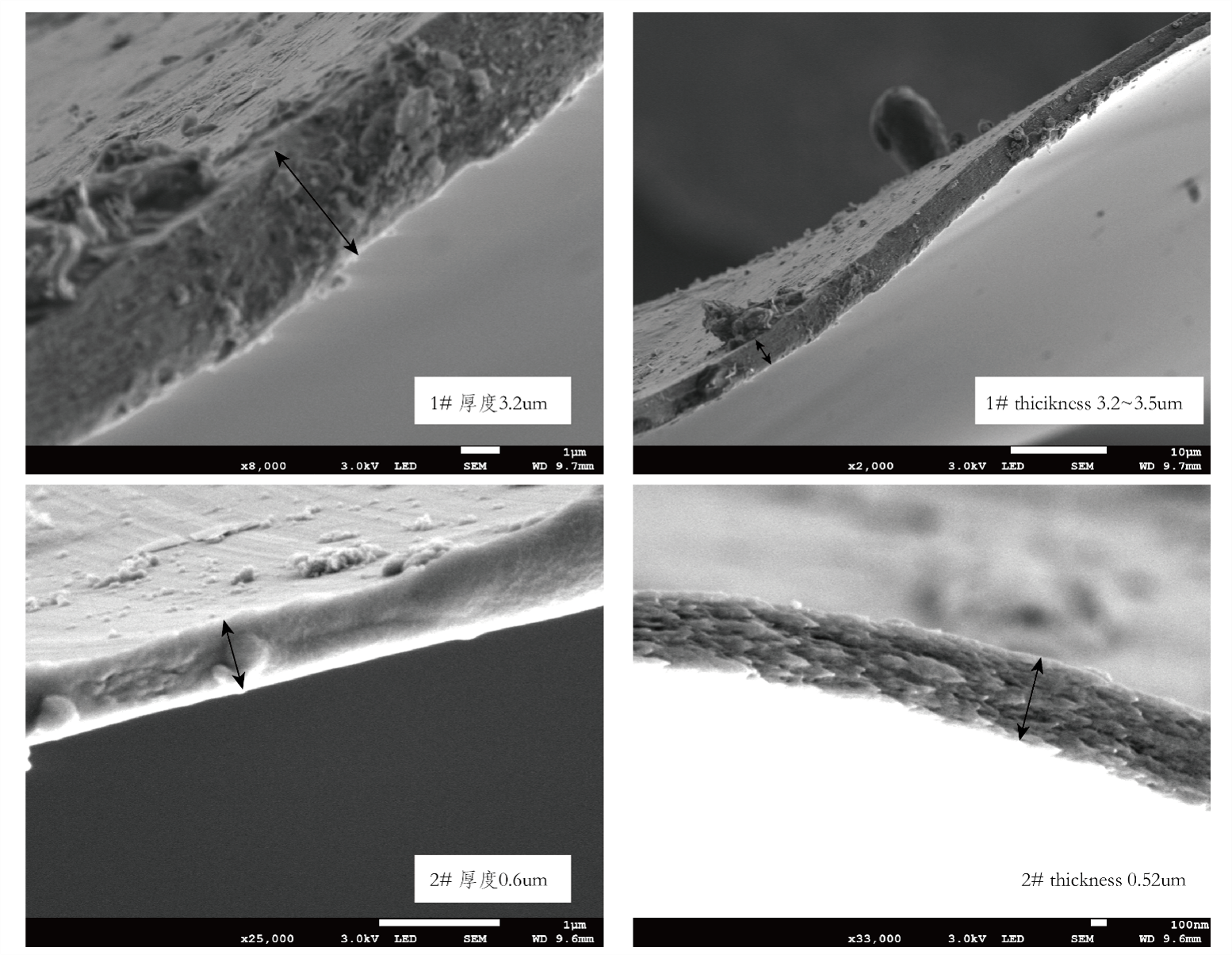
Pumo Spectrum offers an ultrathin PI window film with a thickness of less than 0.6 µm. This film is four times stronger than traditional polypropylene films and efficiently transmits very soft X-rays. A 20 nm-thick aluminum layer is coated onto the film surface to impart conductivity, making it suitable for constructing the electric field required for flow proportional detectors. The figure below shows an electron microscope cross-section of the ultrathin PI window film along with its measured thickness.

Product Overview
-
When measuring Be, B, C, N, O, and F elements using X-ray fluorescence spectroscopy, the characteristic X-ray energies of these elements are extremely low—ranging from 108 eV to 667 eV—and fall within the very soft X-ray region, where they are readily absorbed by materials. To ensure a high transmission rate of these characteristic X-rays and to enhance the detector’s quantum efficiency, an ultrathin conductive window film is typically applied to the detector’s surface.
-
Pumo Spectrum offers an ultrathin PI window film with a thickness of less than 0.6 µm. This film is four times stronger than traditional polypropylene films and efficiently transmits very soft X-rays. A 20 nm-thick aluminum layer is coated onto the film surface to impart conductivity, making it suitable for constructing the electric field required for flow proportional detectors. The figure below shows an electron microscope cross-section of the ultrathin PI window film along with its measured thickness.
-
Anodic bonding technology uses high temperatures and a DC electric field to securely bond silicon with glass containing mobile ions, achieving high bonding strength and excellent interfacial properties. This technology is widely applied in the manufacture of microelectronics, sensors, and semiconductor devices.
-
Pumo Spectrum has mastered this core process and successfully applied it in the production of silicon or germanium bent crystals, demonstrating promising application prospects in the semiconductor field.